目录
0.先验知识
1.测试例介绍
2.总线接口
3.配置信息
5.Neural Networks & Simulations
6.Linux Kernel & Driver Development

RoadMap of NVDLA
0 先验知识
如果你对神经网络不熟悉,或者初次接触神经网络,那么这篇教程会是一个很好的入门资料。
2.深度学习初学者了解CNN卷积神经网络的黄金指南(第二部分)
#Deep Learning回顾#之LeNet、AlexNet、GoogLeNet、VGG、ResNet
谷歌系列 :Inception v1到v4
Google Inception系列【2016-11-10】
还有一些在学习NVDLA过程中,可能会遇到的专业知识,大多数是之前没有碰到的,有的是工具,有的是内核程序。这里列出来,共参考。
GEM/DRM
GEM:GEM stands for Graphics Execution Manager and is a generic DRM memory-management framework in the kernel, that is used by many different drivers. Gem is designed to manage graphics memory, control access to the graphics device execution context and handle essentially NUMA environment unique to modern graphics hardware. Gem allows multiple applications to share graphics device resources without the need to constantly reload the entire graphics card. Data may be shared between multiple applications with gem ensuring that the correct memory synchronization occurs.
Read more at: https://www.commandlinux.com/man-page/man7/drm-gem.7.html
Google Protocol Buffer
Google Protocol Buffer( 简称 Protobuf) 是 Google 公司内部的混合语言数据标准,目前已经正在使用的有超过 48,162 种报文格式定义和超过 12,183 个 .proto 文件。他们用于 RPC 系统和持续数据存储系统。
Protocol Buffers 是一种轻便高效的结构化数据存储格式,可以用于结构化数据串行化,或者说序列化。它很适合做数据存储或 RPC 数据交换格式。可用于通讯协议、数据存储等领域的语言无关、平台无关、可扩展的序列化结构数据格式。目前提供了 C++、Java、Python 三种语言的 API。
Google Protocol Buffer 的使用和原理IBM的教程
1 测试例介绍
1.1 基本测试
1.1.1 sanity0
基本的寄存器读写,先写后读,比较写后读的结果是否一致。
1.1.2. sanity1
存储器传输,使用BDMA将数据从dbb复制到dbb,通过轮训寄存器来判断结束。
1.1.3. sanity2
与sanity1类似,换成使用中断方式判断结束。
1.1.4. sanity3
卷积测试。使用轮训寄存器判断结束,并比较输出存储器结果。
1.1.5. sanity3_cvsram
与sanity3类似,存储器换成cvsram通路。
1.2. 单功能测试
1.2.1. conv_8x8_fc_int16
完成一个卷积层(全连接层-fully-connected layer)的计算,数据类型为int16,输入特征为8x8x32,权值为16个8x8x32的向量,输出为16个int16的数值。具体可参见介绍CMAC的小节。
1.2.2. pdp_max_pooling_int16
1.2.3. sdp_relu_int16
1.3. 实例功能测试
1.3.1. googlenet_conv2_3x3_int16(30min)
1.3.2. cc_alexnet_conv5_relu5_int16_dtest_cvsram(156min)
完成AlexNet的卷积层/ReLU层的操作。输入为13x13x384,权值为256个3x3x384的向量。
1.3 测试格式
支持cpu寄存器读/写、mem读/写、mem加载(load)/转储(dump)、中断等待等7条命令。
CSB_MASTER从文件input.txn中读取指令(包括一系列寄存器、存储器访问指令),脚本文件synth_tb/inp_txn_to_hexdump.pl将input.txn转成类似于指令二进制码形式input.txn.raw以供CSB_MATER_SEQ读取并执行。

一个input.txn的示例
1.3.1. write_reg
write_reg <misc:16><addr:16><data:32>
将32位数据写入16位地址中。
Bit17:1-CSB MASTER等待wr_complete或者ERROR才发出下一条读写命令;0-不等待。
Bit16:1-write,0-read
1.3.2. read_reg
read_reg <misc:16><addr:16><bitmask:32><expectedData:32>
从16位地址中读取32位数据,与期望值进行比较。轮训寄存器,轮训次数由+read_reg_poll_retries决定,默认50。
1.3.3. write_mem
write_mem <addr:64><bytemask:16><wdata:128>
将128位数据写入64位地址中,带16比特字节掩码。
1.3.4. read_mem
read_mem <addr:64><bitmask:128><expectedData: 128>
与read_reg类似,轮询方式读写。
1.3.5. load_mem/dump_mem
load_mem <addr:64><num_bytes:32><string>
dump_mem <addr:64><num_bytes:32><sting>
分别使用Verilog的系统调用进程$readmemh()和$writememh()完成数据直接从文件中读取或者写入。提升仿真速度。
1.3.6. wait
四种中断方式,wait high/low/posedge/negedge dla_intr
1.4. 结束
还有一些其他的测试参数,可以参考nvdla.org/integration_guide.html。
2. 总线接口
NVDLA的顶层接口包括控制总线,数据总线以及时钟复位和中断信号,比较简洁。控制总线CSB遵循简单地握手协议,而数据总线则采用简化版的AXI4.0协议。
2.1. Configuration Space Bus
控制总线CSB,即Configuration Space Bus,主要包括请求通道,读数据通道和写响应通道,包括12组信号线,具体信号线个数与所选择的AXI总线位宽有关。

请求通道,Request Channel,主要完成CSB Master对NVDLA的读写操作。其支持简单的valid/ready握手协议,地址位宽固定为16比特,数据位宽固定为32比特,且不支持burst操作,各个读写命令之间相互独立,不支持乱序完成和发射。

读数据通道,Read Data Channel,主要返回CSB Master读请求命令的数据,valid为高时,数据有效。也不支持乱序响应。

写响应通道,Write Response Channel,也遵循valid协议,针对no-posted模式,返回写响应信号,同时也不支持乱序响应。

下图是一个简单的两写两读的时序图,第二个写操作为no-posted模式。

2.2. Data Bus
NVDLA的存储器接口比较简单,采用了简化版的AXI4.0协议,比如支持的burst类型仅为Incr类型,且burstsize也与数据位宽对齐,保持一致等。

同时为了隐藏配置NVDLA寄存器带来的延迟和增加的神经网络处理时间,NVDLA采用了ping-pong寄存器模式,在group0寄存器工作的同时,CSB Master可以配置下一层的group1寄存器。这里需要注意的是,为了简化硬件设计,NVDLA子模块间的工作时序以及启动的依赖关系,都是由软件负责,这也与TPU相类似。可见,仅流片NVDLA,是没有任何实际意义的。

3. 配置信息
NVDLA的硬件参数列表,用户可以通过合理设置在面积、功耗和性能之间取得最佳组合。
| 序号 | 名称 | 可选项 | 备注 | |
|---|---|---|---|---|
| 001 | Data Type | B/int4/int8/int16/int32/fp16/fp32/fp64 | 功能模块支持的数据类型 | |
| 002 | Input image memory formats | Planar images/semi-planar images/other format | ||
| 003 | Weight compression | |||
| 004 | Winograd convolution | |||
| 005 | Batched convolution | |||
| 006 | Convolution buffer size | bank-num:2-32,bank-size:4KiB-8KiB | ||
| 007 | MAC array size | C:8-64;K:4-64 | ||
| 008 | Second memory interface | SRAM接口 | ||
| 009 | Non-linear activation functions | 非线性函数,LUT实现 | ||
| 010 | Activation engine size | 每拍输出个数1-16 | ||
| 011 | Bridge DMA engine | |||
| 012 | Data reshape engine | |||
| 013 | Pooling engine size | 1-4 | ||
| 014 | Pooling engine presence | |||
| 015 | Local response normalization engine presence | |||
| 016 | Local response normalization engine size | 每拍输出1-4 | ||
| 017 | Memory interface bit width | |||
| 018 | Memory read latency tolerance |
NVDLA的配置寄存器需要256KiB的MMIO地址空间。CSB接口的起始地址(在系统实现的时候需要加上基地址,此处为偏移地址)为0x0000_0000,每个子模块的配置寄存器地址4KiB对齐。其中,CBUF没有配置寄存器。
对于某些配置,可能不包括一些子模块,诸如SDP、PDP、CDP等,其配置寄存器的地址空间则处于保留状态,且不能访问。
- For NV_LARGE Memory Map
| DLA Sub-unit | Start Address | End Address | Size(KiB) |
|---|---|---|---|
| CFGROM | 0x0000_0000 | 0x0000_0FFF | 4 |
| GLB | 0x0000_1000 | 0x0000_1FFF | 4 |
| MCIF | 0x0000_2000 | 0x0000_2FFF | 4 |
| SRAMIF | 0x0000_3000 | 0x0000_3FFF | 4 |
| CDMA | 0x0000_4000 | 0x0000_4FFF | 4 |
| CSC | 0x0000_5000 | 0x0000_5FFF | 4 |
| CMAC_A | 0x0000_6000 | 0x0000_6FFF | 4 |
| CMAC_B | 0x0000_7000 | 0x0000_7FFF | 4 |
| CACC | 0x0000_8000 | 0x0000_8FFF | 4 |
| SDP_RDMA | 0x0000_9000 | 0x0000_9FFF | 4 |
| SDP | 0x0000_A000 | 0x0000_AFFF | 4 |
| PDP_RDMA | 0x0000_B000 | 0x0000_BFFF | 4 |
| PDP | 0x0000_C000 | 0x0000_CFFF | 4 |
| CDP_RDMA | 0x0000_D000 | 0x0000_DFFF | 4 |
| CDP | 0x0000_E000 | 0x0000_EFFF | 4 |
| BDMA | 0x0000_F000 | 0x0000_FFFF | 4 |
| RUBIK | 0x0001_0000 | 0x0001_0FFF | 4 |
Total 68KB.
- For NV_SMALL Memory Map
| DLA Sub-unit | Start Address | End Address | Size(KiB) |
|---|---|---|---|
| CFGROM | 0x0000_0000 | 0x0000_0FFF | 4 |
| GLB | 0x0000_1000 | 0x0000_1FFF | 4 |
| MCIF | 0x0000_2000 | 0x0000_2FFF | 4 |
| CDMA | 0x0000_3000 | 0x0000_3FFF | 4 |
| CSC | 0x0000_4000 | 0x0000_4FFF | 4 |
| CMAC_A | 0x0000_5000 | 0x0000_5FFF | 4 |
| CMAC_B | 0x0000_6000 | 0x0000_6FFF | 4 |
| CACC | 0x0000_7000 | 0x0000_7FFF | 4 |
| SDP_RDMA | 0x0000_8000 | 0x0000_8FFF | 4 |
| SDP | 0x0000_9000 | 0x0000_9FFF | 4 |
| PDP_RDMA | 0x0000_A000 | 0x0000_AFFF | 4 |
| PDP | 0x0000_B000 | 0x0000_BFFF | 4 |
| CDP_RDMA | 0x0000_C000 | 0x0000_CFFF | 4 |
| CDP | 0x0000_D000 | 0x0000_DFFF | 4 |
Total 56KB.
- For NV_SMALL_256 Memory Map
3.1 CDMA配置寄存器
CDMA作为Convolution流水线的一环,从SRAM和DRAM中读取数据,并存入CBUF中。CDMA支持多种格式的数据输入,包括Pixel data /Feature data /Uncompressed/compressed weight /WMB /WGS等。CDMA具有两个读通道,AXI接口协议,分别完成数据和权值的读取。CDMA的只发出读请求,且64位对齐访问。
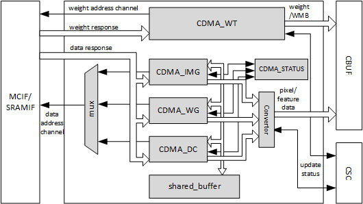
在CDMA的内部,存在4个子模块,分别为CDMA_DC,CDMA_WG,CDMA_IMG和一个权值读取模块CDMA_WT,每个子模块的工作流程一样,只不过数据在存入CBUF的时候顺序不同而已;且某一时刻只有一个子模块处于工作状态。
CDMA的工作成流程大致如下:
- 1.检查CBUF是否有足够的剩余空间存放读取的数据
- 2.发起读数据请求
- 3.将数据暂存在共享存储器中
- 4.根据配置,将数据的顺序重新摆放
- 5.发起CBUF的写入请求
- 6.将整理后的数据写入CBUF
- 7.更新CBUF的相关状态寄存器,以供CDMA查阅
3.1.1 寄存器描述
| Name | Address | Bits Function | Description |
|---|---|---|---|
| S_STATUS | 0x5000 | [17:16]-status1;[1:0]-status0 | Idle status of two register groups |
| S_POINTER | 0x5004 | [16]-consumer;[0]-producer | Pointer for CSB master and data path to access groups |
| S_ARBITER | 0x5008 | [19:16]-arb_wmb;[3:0]-arb_weight | WMB and Weight share same port to access external memory.This register controls the weight factor in the arbiter. |
| S_CBUF_FLUSH_STATUS | 0x500c | [0]-flush_done | Indicates whether CBUF flush is finished after reset. |
| D_OP_ENABLE | 0x5010 | — | Set it to 1 to kick off operation for current register group |
| D_MISC_CFG | 0x5014 | [29]-skip_weight_rls;[24]-skip_data_rls;[20]-weight_reuse;[16]-data_reuse;[13:12]-proc_precison;[5:4]-in_precison;[0]-conv_mode | Configuration of operation: convolution mode, precision, weight reuse, data reuse. |
| D_DATAIN_FORMAT | 0x5018 | [16]-pixel_sign_override;[12]-pixel_mapping;[9:8]-pixel_format;[0]-datain_format | Input data format and pixel format |
| D_DATAIN_SIZE_0 | 0x501c | [28:16]-height;[12:0]-width | Input cube’s width and height |
| D_DATAIN_SIZE_1 | 0x5020 | [12:0]-channel | Input cube’s channel |
| D_DATAIN_SIZE_EXT_0 | 0x5024 | [28:16]-height_ext;[12:0]-width_ext | Input cube’s width and height after extension |
| D_PIXEL_OFFSET | 0x5028 | [18:16]-y_offset;[4:0]-x_offset | For image-in mode, horizontal offset and vertical offset of the 1 st pixel. |
| D_DAIN_RAM_TYPE | 0x502c | [0]-type | Ram type of input RAM |
| D_DAIN_ADDR_HIGH_0 | 0x5030 | [31:0]-high_addr | Higher 32bits of input data address when axi araddr is 64bits |
| D_DAIN_ADDR_LOW_0 | 0x5034 | [31:0]-low_addr | Lower 32bits of input data address |
| D_DAIN_ADDR_HIGH_1 | 0x5038 | [31:0]-high_addr | Higher 32bits of input data address of UV plane when axi araddr is 64bits |
| D_DAIN_ADDR_LOW_1 | 0x503c | [31:0]-low_addr | Lower 32bits of input data address of UV plane |
| D_LINE_STRIDE | 0x5040 | [31:0]-line_stride | Line stride of input cube |
| D_LINE_UV_STRIDE | 0x5044 | [31:0]-uv_stride | Line stride of input cube’s UV plane |
| D_SURF_STRIDE | 0x5048 | [31:0]-surf_stride | Surface stride of input cube |
| D_DAIN_MAP | 0x504c | [16]-surf_packed;[0]-line_packed | Whether input cube is line packed or surface packed |
| RESERVED | 0x5050 | — | This address is reserved |
| RESERVED | 0x5054 | — | This address is reserved |
| D_BATCH_NUMBER | 0x5058 | [4:0]-batch_num | Number of batches |
| D_BATCH_STRIDE | 0x505c | [31:0]-batch_stride | The stride of input data cubes when batches > 1 |
| D_ENTRY_PER_SLICE | 0x5060 | [13:0]-entry_per_slice | Number of CBUF entries used for one input slice |
| D_FETCH_GRAIN | 0x5064 | [11:0]-fetch_grain | Number of slices to be fetched before sending update information to CSC |
| D_WEIGHT_FORMAT | 0x5068 | [0]-weight_format | Whether weight is compressed or not |
| D_WEIGHT_SIZE_0 | 0x506c | [17:0]-kernel_bytes | The size of one kernel in bytes |
| D_WEIGHT_SIZE_1 | 0x5070 | [12:0]-kernel_num | Number of kernels |
| D_WEIGHT_RAM_TYPE | 0x5074 | [0]-ram_type | Ram type of weight |
| D_WEIGHT_ADDR_HIGH | 0x5078 | [31:0]-high_addr | Higher 32bits of weight address when axi araddr is 64bits |
| D_WEIGHT_ADDR_LOW | 0x507c | [31:0]-low_addr | Lower 32bits of weight address |
| D_WEIGHT_BYTES | 0x5080 | [31:0]-weight_bytes | Total bytes of Weight |
| D_WGS_ADDR_HIGH | 0x5084 | [31:0]-high_addr | Higher 32bits of wgs address when axi araddr is 64bits |
| D_WGS_ADDR_LOW | 0x5088 | [31:0]-low_addr | Lower 32bits of wgs address |
| D_WMB_ADDR_HIGH | 0x508c | [31:0]-high_addr | Higher 32bits of wmb address when axi araddr is 64bits |
| D_WMB_ADDR_LOW | 0x5090 | [31:0]-low_addr | Lower 32bits of wmb address |
| D_WMB_BYTES | 0x5094 | [27:0]-wmb_bytes | Total bytes of WMB |
| D_MEAN_FORMAT | 0x5098 | [0]-mean_format | Whether mean registers are used or not |
| D_MEAN_GLOBAL_0 | 0x509c | [31:16]-mean_gu;[15:0]-mean_ry | Global mean value for red in RGB or Y in YUV Global mean value for green in RGB or U in YUV |
| D_MEAN_GLOBAL_1 | 0x50a0 | [31:16]-mean_ax;[15:0]-mean_by | Global mean value for blue in RGB or V in YUV Global mean value for alpha in ARGB/AYUV or X in XRGB |
| D_CVT_CFG | 0x50a4 | [9:4]-cvt_truncate;[0]-cvt_en | Enable/disable input data converter in CDMA and number of bits to be truncated in the input data converter |
| D_CVT_OFFSET | 0x50a8 | [15:0]-cvt_offset | Offset of input data convertor |
| D_CVT_SCALE | 0x50ac | [15:0]-cvt_scale | Scale of input data convertor |
| D_CONV_STRIDE | 0x50b0 | [18:16]-conv_y_stride;[2:0]-conv_x_stride | Convolution x stride and convolution y stride |
| D_ZERO_PADDING | 0x50b4 | [29:24]-bottom;[20:16]-top;[13:8]-right;[4:0]-left | Left/right/top/bottom padding size |
| D_ZERO_PADDING_VALUE | 0x50b8 | [15:0]-pad_value | Padding value |
| D_BANK | 0x50bc | [20:16]-weight_bank;[4:0]-data_bank | Number of data banks and weight banks in CBUF |
| D_NAN_FLUSH_TO_ZERO | 0x50c0 | [0]-flush_to_zero | Enable/Disable flushing input NaN to zero |
| D_NAN_INPUT_DATA_NUM | 0x50c4 | [31:0]-read_only | Count NaN number in input data cube, update per layer |
| D_NAN_INPUT_WEIGHT_NUM | 0x50c8 | [31:0]-read_only | Count NaN number in weight kernels, update per layer |
| D_INF_INPUT_DATA_NUM | 0x50cc | [31:0]-read_only | Count infinity number in input data cube, update per layer |
| D_INF_INPUT_WEIGHT_NUM | 0x50d0 | [31:0]-read_only | Count infinity number in weight kernels, update per layer |
| D_PERF_ENABLE | 0x50d4 | [0]-perf_en | Enable/disable performance counter |
| D_PERF_DAT_READ_STALL | 0x50d8 | [31:0]-read_only | Count blocking cycles of read request of input data, update per layer |
| D_PERF_WT_READ_STALL | 0x50dc | [31:0]-read_only | Count blocking cycles of read request of weight data, update per layer |
| D_PERF_DAT_READ_LATENCY | 0x50e0 | [31:0]-read_only | Count total latency cycles of read response of input data, update per layer |
| D_PERF_WT_READ_LATENCY | 0x50e4 | [31:0]-read_only | Count total latency cycles of read request of weight data, update per layer |
| D_CYA | 0x50e8 | — | — |
3.1.2 使用示例
3.2 CACC配置寄存器
CACC主要负责部分和的累加计算,在卷积层和全连接层的时候会用到,其接收CMAC模块的输出,计算结果作为SDP的输入。在将计算结果送入SDP之前,需要进行round和饱和处理,对于INT16的情况下输出48bit,INT8则输出34bit;而在CACC和SDP之间传输的位宽为32bit;具体的round算法则由寄存器D_CLIP_CFG的相应位CLIP_TRUNCATE决定;对于浮点FP16来说,则直接将FP48转换成FP32输出。其配置寄存器地址空间为0x9000-0x9fff(且与具体配置有关).同时,CACC内部集成大容量的缓存,有助于提高卷积流水线的数据吞吐。

如图所示,CACC包括组装单元和发送单元,还包括加法器阵列和截断饱和阵列单元,以及流量控制单元和检查模块。CACC的工作流程为:
- 从部分和暂存单元(组装单元)中进行数据预取
- 预取完成,将部分和送入加法器阵列进行累加;如果是初次计算,则部分和为0
- 收集累加和
- 将新生产的累加和送入暂存单元
- 重复1-3步,直到一个通道的数据完成
- 将本通道的计算结果进行饱和处理
- 将不同通道的数据送入发送单元的缓存区
- 将结果送入SDP单元
加法器阵列包括64个INT48单元,64个INT34单元,和64个FP48单元。在不同模式,可以激活不同个数的加法器进行运算,其精确度如下表所示。
| Input Format | Accumulative Sum | Truncated Result |
|---|---|---|
| INT8 | INT34 | INT32 |
| INT16 | INT48 | INT32 |
| FP16 | FP44 (8b exponent, 38b signed decimal) | FP32 (IEEE754 standard) |
组装单元(即部分和暂存单元)包括4个96Bx32的SRAM单元和4个64Bx32的SRAM单元。在不同的模式下,可以组合成不同的存储位宽和深度,如下表所示。完成一次存取操作,至少需要11拍。
| Input Format and Mode | Activated INT48 Adders | Activated INT34 Adders | Activated FP44 Adders |
|---|---|---|---|
| INT8 DC/Image | Adder 0~15 | Adder 0~15 | NA |
| INT8 Winograd | Adder 0~63 | Adder 0~63 | NA |
| INT16 DC/Image | Adder 0~15 | NA | NA |
| INT16 Winograd | Adder 0~63 | NA | NA |
| FP16 DC/Image | NA | NA | Adder 0~15 |
| FP16 Winograd | NA | NA | Adder 0~63 |
| 卷积模式 | INT8 | INT16/FP16 |
|---|---|---|
| DC | 136Bx128 | 96Bx128 |
| Winograd | 544Bx32 | 384Bx32 |
对于发送单元的SRAM,则就包括8个64Bx32的存储阵列。每拍可输入16-128个数据结果,而输出则固定为16个。
CACC也支持Multi-Batch操作,具体可以参考官方说明文档。
3.2.1 寄存器描述
| Name | Address | Bits Function | Description |
|---|---|---|---|
| S_STATUS | 0x9000 | – | Idle status of two register groups |
| S_POINTER | 0x9004 | – | Pointer for CSB master and data path to access groups |
| D_OP_ENABLE | 0x9008 | – | Set it to 1 to kick off operation for current register group |
| D_MISC_CFG | 0x900c | [0]-conv_mode;[13:12]-proc_precision | Configuration of operation: convolution mode, precision, etc. |
| D_DATAOUT_SIZE_0 | 0x9010 | [12:0]-dataout_width;[28:16]-dataout_height | Input cube’s width and height after extension |
| D_DATAOUT_SIZE_1 | 0x9014 | [12:0]-dataout_channel | Input cube’s channel after extension |
| D_DATAOUT_ADDR | 0x9018 | [31:5]-dataout_addr | Address of output cube |
| D_BATCH_NUMBER | 0x901c | [4:0]-batches | Number of batches |
| D_LINE_STRIDE | 0x9020 | [23:5]-line_stride | Line stride of output cube |
| D_SURF_STRIDE | 0x9024 | [23:5]-surf_stride | Line stride of surface cube |
| D_DATAOUT_MAP | 0x9028 | [0]-line_packed;[16]-surf_packed | Whether output cube is line packed or surface packed |
| D_CLIP_CFG | 0x902c | [4:0]-clip_truncate | Number of bits to be truncated before sending to SDP |
| D_OUT_SATURATION | 0x9030 | – | Output saturation count |
| D_CYA | 0x9034 | ??? | ??? |
3.2.2 使用示例
在BVLC的model zoo中,lenet的实现是跟原始版本不一样的,在BVLC版本的Lenet中,存在四处使用CACC的地方,分别是卷积层1和卷积层2,以及全连接层1和全连接层2.对于配置寄存器中dataout相关信息的配置分别如下:
| Num. | dataout_width | dataout_height | dataout_channel |
|---|---|---|---|
| 1 | 0x17 | 0x17 | 0x13 |
| 2 | 0x7 | 0x7 | 0x31 |
| 3 | 0x0 | 0x0 | 0x1f3 |
| 4 | 0x0 | 0x0 | 0x9 |
分别表示卷积层的输出为20x24x24和50x8x8,以及全连接层的输出为500x1x1和10x1x1.
3.3 CMAC配置寄存器
NVDLA的CMAC在实现的时候,为了进行物理设计优化,分为CMAC_A和CMAC_B,因此配置寄存器也是分为两部分。但是两部分的配置寄存器和功能都是一样的。

在winograd模式下,CMAC还完成POA的操作。CMAC单元内部集成了16个相同的子模块,成为CMAC Cell。每个CMAC Cell包括64个16bit乘累加器,支持int16和FP16计算,且包括72个加法器,完成POA操作。对于int8计算,每个计算部件可以分成2个。CMAC计算单元包括7级流水。
CMAC内部还包括了一个状态流水线,采用bypass模式,4拍完成输出。
3.3.1 寄存器描述
- CMAC_A Registers
| Name | Address | Bits Function | Description |
|---|---|---|---|
| S_STATUS | 0x7000 | — | Idle status of two register groups |
| S_POINTER | 0x7004 | —- | Pointer for CSB master and data path to access groups |
| D_OP_ENABLE | 0x7008 | — | Set it to 1 to kick off operation for current register group |
| D_MISC_CFG | 0x700c | [0]-conv_mode;[13:12]-proc_precision | Configuration of operation: convolution mode, precision, etc. |
- CMAC_B Registers
| Name | Address | Bits Function | Description |
|---|---|---|---|
| S_STATUS | 0x8000 | — | Idle status of two register groups |
| S_POINTER | 0x8004 | —- | Pointer for CSB master and data path to access groups |
| D_OP_ENABLE | 0x8008 | — | Set it to 1 to kick off operation for current register group |
| D_MISC_CFG | 0x800c | [0]-conv_mode;[13:12]-proc_precision | Configuration of operation: convolution mode, precision, etc. |
3.4 CSC配置寄存器
3.4.1 寄存器描述
| Name | Address | Bits Function | Description |
|---|---|---|---|
| S_STATUS | 0x6000 | — | Idle status of two register groups |
| S_POINTER | 0x6004 | — | Pointer for CSB master and data path to access groups |
| D_OP_ENABLE | 0x6008 | — | Set it to 1 to kick off operation for current register group |
| D_MISC_CFG | 0x600c | [0]-conv_mode;[9:8]-in_precision;[13:12]-proc_precision;[16]-data_reuse;[20]-weight_reuse;[24]-skip_data_rls;[28]-skip_weight_rls | Configuration of operation: convolution mode, precision, weight reuse, data reuse. |
| D_DATAIN_FORMAT | 0x6010 | [0]-datain_format | Input data format and pixel format |
| D_DATAIN_SIZE_EXT_0 | 0x6014 | [12:0]-datain_width_ext;[28:16]-datain_height_ext; | Input cube’s width and height after extension |
| D_DATAIN_SIZE_EXT_1 | 0x6018 | [12:0]-datain_channel_ext | Input cube’s channel after extension |
| D_BATCH_NUMBER | 0x601c | [4:0]-batches | Number of batches |
| D_POST_Y_EXTENSION | 0x6020 | [1:0]-y_extension | Post extension parameter for image-in |
| D_ENTRY_PER_SLICE | 0x6024 | [11:0]-entries | Number of CBUF entries used for one input slice |
| D_WEIGHT_FORMAT | 0x6028 | [0]-weight_format | Whether weight is compressed or not |
| D_WEIGHT_SIZE_EXT_0 | 0x602c | [4:0]-weight_width_ext;[20:16]-weight_height_ext | Weight’s width and height after extension |
| D_WEIGHT_SIZE_EXT_1 | 0x6030 | [12:0]-weight_channel_ext;[28:16]-weight_kernel | Weight’s channel after extension and number of weight kernels |
| D_WEIGHT_BYTES | 0x6034 | [31:7]-weight_bytes | Total bytes of Weight |
| D_WMB_BYTES | 0x6038 | [27:7]-wmb_bytes | Total bytes of WMB |
| D_DATAOUT_SIZE_0 | 0x603c | [12:0]-dataout_width;[28:16]-dataout_height; | Output cube’s width and height |
| D_DATAOUT_SIZE_1 | 0x6040 | [12:0]-dataout_channel | Output cube’s channel |
| D_ATOMICS | 0x6044 | [20:0]-atomics | Equals to output_data_cube_width * output_data_cube_height - 1 |
| D_RELEASE | 0x6048 | [11:0]-rls_slices | Slices of CBUF to be released at the end of current layer |
| D_CONV_STRIDE_EXT | 0x604c | [2:0]-conv_x_stride_ext;[18:16]-conv_y_stride_ext | Convolution x stride and convolution y stride after extension |
| D_DILATION_EXT | 0x6050 | [4:0]-x_dilation_ext;[20:16]-y_dilation_ext | Dilation parameter |
| D_ZERO_PADDING | 0x6054 | [4:0]-pad_left;[20:16]-pad_top | Left/right/top/bottom padding size |
| D_ZERO_PADDING_VALUE | 0x6058 | [15:0]-pad_value | Padding value |
| D_BANK | 0x605c | [3:0]-data_bank;[19:16]-weight_bank | Number of data banks and weight banks in CBUF |
| D_PRA_CFG | 0x6060 | [1:0]-pra_truncate | PRA truncate in Winograd mode, range: 0~2 |
| D_CYA | 0x6064 | — | CYA ??? |
3.4.2 使用示例
在BVLC的model zoo中,lenet的实现是跟原始版本不一样的,在BVLC版本的Lenet中,存在四处使用CACC的地方,分别是卷积层1和卷积层2,以及全连接层1和全连接层2。为了使得文档简洁,这里只针对conv1层中所使用的weight和datain的配置信息分别如下:
| Num. | datain_width | datain_height | datain_channel |
|---|---|---|---|
| 1 | 0x1b | 0x1b | 0x0 |
| 2 | 0xb | 0xb | 0x13 |
| 3 | 0x3 | 0x3 | 0x31 |
| 4 | 0x0 | 0x0 | 0x1f3 |
可以看出跟CACC的输出正好是相对应的关系。
| Num. | weight_width_ext | weight_height_ext | weight_channel_ext | weight_kernel |
|---|---|---|---|---|
| 1 | 0x4 | 0x4 | 0x0 | 0x13 |
| 2 | 0x4 | 0x4 | 0x13 | 0x31 |
| 3 | 0x3 | 0x3 | 0x31 | 0x1f3 |
| 4 | 0x0 | 0x0 | 0x1f3 | 0x9 |
3.5 SDP配置寄存器
3.5.1 寄存器描述
| Name | Address | Bits Function | Description |
|---|---|---|---|
| S_STATUS | 0xb000 | Idle status of two register groups | |
| S_POINTER | 0xb004 | Pointer for CSB master and data path to access groups | |
| S_LUT_ACCESS_CFG | 0xb008 | LUT access address and type | |
| S_LUT_ACCESS_DATA | 0xb00c | Data register of read or write LUT | |
| S_LUT_CFG | 0xb010 | LUT’s type: exponent or linear. And the selection between LE and LO tables. | |
| S_LUT_INFO | 0xb014 | LE and LO LUT index offset and selection | |
| S_LUT_LE_START | 0xb018 | Start of LE LUT’s range | |
| S_LUT_LE_END | 0xb01c | End of LE LUT’s range | |
| S_LUT_LO_START | 0xb020 | Start of LO LUT’s range | |
| S_LUT_LO_END | 0xb024 | End of LO LUT’s range | |
| S_LUT_LE_SLOPE_SCALE | 0xb028 | Slope scale parameter for LE LUT underflow and overflow, signed value | |
| S_LUT_LE_SLOPE_SHIFT | 0xb02c | Slope shift parameter for LE_LUT underflow and overflow, signed value | |
| S_LUT_LO_SLOPE_SCALE | 0xb030 | Slope scale parameter for LO LUT underflow and overflow, signed value | |
| S_LUT_LO_SLOPE_SHIFT | 0xb034 | Slope shift parameter for LO_LUT underflow and overflow, signed value | |
| D_OP_ENABLE | 0xb038 | Set it to 1 to kick off operation for current register group | |
| D_DATA_CUBE_WIDTH | 0xb03c | Input cube’s width | |
| D_DATA_CUBE_HEIGHT | 0xb040 | Input cube’s height | |
| D_DATA_CUBE_CHANNEL | 0xb044 | Input cube’s channel | |
| D_DST_BASE_ADDR_LOW | 0xb048 | Lower 32bits of output data address | |
| D_DST_BASE_ADDR_HIGH | 0xb04c | Higher 32bits of output data address when axi awaddr is 64bits | |
| D_DST_LINE_STRIDE | 0xb050 | Line stride of output data cube | |
| D_DST_SURFACE_STRIDE | 0xb054 | Surface stride of output data cube | |
| D_DP_BS_CFG | 0xb058 | Configurations of BS module: bypass, algorithm, etc. | |
| D_DP_BS_ALU_CFG | 0xb05c | Source type and shifter value of BS ALU | |
| D_DP_BS_ALU_SRC_VALUE | 0xb060 | Operand value of BS ALU | |
| D_DP_BS_MUL_CFG | 0xb064 | Source type and shifter value of BS MUL | |
| D_DP_BS_MUL_SRC_VALUE | 0xb068 | Operand value of BS MUL | |
| D_DP_BN_CFG | 0xb06c | Configurations of BN module: bypass, algorithm, etc. | |
| D_DP_BN_ALU_CFG | 0xb070 | Source type and shifter value of BN ALU | |
| D_DP_BN_ALU_SRC_VALUE | 0xb074 | Operand value of BN ALU | |
| D_DP_BN_MUL_CFG | 0xb078 | Source type and shifter value of BN MUL | |
| D_DP_BN_MUL_SRC_VALUE | 0xb07c | Operand value of BN MUL | |
| D_DP_EW_CFG | 0xb080 | Configurations of EW module: bypass, algorithm, etc. | |
| D_DP_EW_ALU_CFG | 0xb084 | Source type and bypass control of EW ALU | |
| D_DP_EW_ALU_SRC_VALUE | 0xb088 | Operand value of EW ALU | |
| D_DP_EW_ALU_CVT_OFFSET_VALUE | 0xb08c | Converter offset of EW ALU | |
| D_DP_EW_ALU_CVT_SCALE_VALUE | 0xb090 | Converter scale of EW ALU | |
| D_DP_EW_ALU_CVT_TRUNCATE_VALUE | 0xb094 | Converter truncate of EW ALU | |
| D_DP_EW_MUL_CFG | 0xb098 | Source type and bypass control of EW MUL | |
| D_DP_EW_MUL_SRC_VALUE | 0xb09c | Operand value of EW MUL | |
| D_DP_EW_MUL_CVT_OFFSET_VALUE | 0xb0a0 | Converter offset of EW MUL | |
| D_DP_EW_MUL_CVT_SCALE_VALUE | 0xb0a4 | Converter scale of EW MUL | |
| D_DP_EW_MUL_CVT_TRUNCATE_VALUE | 0xb0a8 | Converter truncate of EW MUL | |
| D_DP_EW_TRUNCATE_VALUE | 0xb0ac | Truncate of EW | |
| D_FEATURE_MODE_CFG | 0xb0b0 | Operation configuration: flying mode, output destination, Direct or Winograd mode, flush NaN to zero, batch number. | |
| D_DST_DMA_CFG | 0xb0b4 | Destination RAM type | |
| D_DST_BATCH_STRIDE | 0xb0b8 | Stride of output cubes in batch mode | |
| D_DATA_FORMAT | 0xb0bc | Data precision | |
| D_CVT_OFFSET | 0xb0c0 | Output converter offset | |
| D_CVT_SCALE | 0xb0c4 | Output converter scale | |
| D_CVT_SHIFT | 0xb0c8 | Output converter shifter value | |
| D_STATUS | 0xb0cc | Output of equal mode | |
| D_STATUS_NAN_INPUT_NUM | 0xb0d0 | Input NaN element number | |
| D_STATUS_INF_INPUT_NUM | 0xb0d4 | Input Infinity element number | |
| D_STATUS_NAN_OUTPUT_NUM | 0xb0d8 | Output NaN element number | |
| D_PERF_ENABLE | 0xb0dc | Enable/Disable performance counting | |
| D_PERF_WDMA_WRITE_STALL | 0xb0e0 | Count stall cycles of write DMA for one layer | |
| D_PERF_LUT_UFLOW | 0xb0e4 | Element number of both table underflow | |
| D_PERF_LUT_OFLOW | 0xb0e8 | Element number of both table overflow | |
| D_PERF_OUT_SATURATION | 0xb0ec | Element number of both table saturation | |
| D_PERF_LUT_HYBRID | 0xb0f0 | Element number of both hit, or both miss situation that element underflow one table and at the same time overflow the other. | |
| D_PERF_LUT_LE_HIT | 0xb0f4 | Element number of only LE table hit | |
| D_PERF_LUT_LO_HIT | 0xb0f8 | Element number of only LO table hit |
3.6 CDP配置寄存器
CDP模块主要完成LRN(Local Response Normalization)的功能,主要是为了侧抑制(Lateral inhibition),侧抑制是神经系统信息处理的基本原则之一,在2012年AlexNet论文中首次用于CNN网络,然而后来研究人员发现(暂时),这一层的功能并不突出,对网络性能的提升作用不大。可以参考these kinds of layers have a minimal impact。
3.6.1 寄存器描述
| Name | Address | Bits Function | Description |
|---|---|---|---|
| S_STATUS | 0xf000 | Idle status of two register groups | |
| S_POINTER | 0xf004 | Pointer for CSB master and data path to access groups | |
| S_LUT_ACCESS_CFG | 0xf008 | [17]-read/write, [16]-Table ID LE/LO, [0-15]-addr | LUT access address and type |
| S_LUT_ACCESS_DATA | 0xf00c | [0-15]-data | Data register of read or write LUT |
| S_LUT_CFG | 0xf010 | LUT’s type: exponent or linear. And the selection between LE and LO tables. | |
| S_LUT_INFO | 0xf014 | LE and LO LUT index offset and selection | |
| S_LUT_LE_START_LOW | 0xf018 | Lower 32bits of start of LE LUT’s range | |
| S_LUT_LE_START_HIGH | 0xf01c | Higher 6bits of start of LE LUT’s range | |
| S_LUT_LE_END_LOW | 0xf020 | Lower 32bits of end of LE LUT’s range | |
| S_LUT_LE_END_HIGH | 0xf024 | Higher 6bits of end of LE LUT’s range | |
| S_LUT_LO_START_LOW | 0xf028 | Lower 32bits of start of LO LUT’s range | |
| S_LUT_LO_START_HIGH | 0xf02c | Higher 6bits of start of LO LUT’s range | |
| S_LUT_LO_END_LOW | 0xf030 | Lower 32bits of end of LO LUT’s range | |
| S_LUT_LO_END_HIGH | 0xf034 | Higher 6bits of end of LO LUT’s range | |
| S_LUT_LE_SLOPE_SCALE | 0xf038 | Slope scale parameter for LE LUT underflow and overflow, signed value | |
| S_LUT_LE_SLOPE_SHIFT | 0xf03c | Slope shift parameter for LE_LUT underflow and overflow, signed value | |
| S_LUT_LO_SLOPE_SCALE | 0xf040 | Slope scale parameter for LO LUT underflow and overflow, signed value | |
| S_LUT_LO_SLOPE_SHIFT | 0xf044 | Slope shift parameter for LO_LUT underflow and overflow, signed value | |
| D_OP_ENABLE | 0xf048 | Set it to 1 to kick off operation for current register group | |
| D_FUNC_BYPASS | 0xf04c | Square sum process bypass control and multiplier after interpolator bypass control | |
| D_DST_BASE_ADDR_LOW | 0xf050 | Lower 32bits of output data address | |
| D_DST_BASE_ADDR_HIGH | 0xf054 | Higher 32bits of output data address when axi awaddr is 64bits | |
| D_DST_LINE_STRIDE | 0xf058 | Line stride of output cube | |
| D_DST_SURFACE_STRIDE | 0xf05c | Surface stride of output cube | |
| D_DST_DMA_CFG | 0xf060 | RAM type of output data cube | |
| D_DST_COMPRESSION_EN | 0xf064 | This register is not used in OpenDLA 1.0 | |
| D_DATA_FORMAT | 0xf068 | Precision of input data | |
| D_NAN_FLUSH_TO_ZERO | 0xf06c | Option to flush input NaN to zero | |
| D_LRN_CFG | 0xf070 | Normalization length | |
| D_DATIN_OFFSET | 0xf074 | Input data convertor offset | |
| D_DATIN_SCALE | 0xf078 | Input data convertor scale | |
| D_DATIN_SHIFTER | 0xf07c | Input data convertor shifter value | |
| D_DATOUT_OFFSET | 0xf080 | Output data convertor offset | |
| D_DATOUT_SCALE | 0xf084 | Output data convertor scale | |
| D_DATOUT_SHIFTER | 0xf088 | Output data convertor shifter value | |
| D_NAN_INPUT_NUM | 0xf08c | input NaN element number | |
| D_INF_INPUT_NUM | 0xf090 | input Infinity element number | |
| D_NAN_OUTPUT_NUM | 0xf094 | output NaN element number | |
| D_OUT_SATURATION | 0xf098 | saturated element number. | |
| D_PERF_ENABLE | 0xf09c | Enable/Disable performance counting | |
| D_PERF_WRITE_STALL | 0xf0a0 | Element number that for both LUT under-flow | |
| D_PERF_LUT_UFLOW | 0xf0a4 | Element number that for both LUT under-flow | |
| D_PERF_LUT_OFLOW | 0xf0a8 | Element number that for both LUT over-flow | |
| D_PERF_LUT_HYBRID | 0xf0ac | Element number that for both LUT miss, one is over-flow and the other is overflow | |
| D_PERF_LUT_LE_HIT | 0xf0b0 | Element number that for LE_lut hit only | |
| D_PERF_LUT_LO_HIT | 0xf0b4 | Element number that for LO_lut hit only |
3.6.2 简述
原始的LRN公式中包括除法和指数计算,对硬件开销需求较大,因此NVDLA采用了查表方式近似实现。
4. 软件栈Software Stack
4.1 编译器和运行时环境介绍
NVDLA的软件栈包括神经网络模型解析器和运行时环境两部分,目前本段文章编辑阶段(2018-1-16),nvdla_sw的仓库结构如下所示。

目前官方提供的都是二进制文件,且编译器只针对nv_full代码和Caffe,后续可能会支持TensorFlow等其他框架,而且根据线路图,会公开相关的源代码。

./nvdla_compiler [-options] –prototxt
./nvdla_runtime [-options] –loadable
where options include:
-h print this help message
-s launch test in server mode
–loadable
–image
–imgshift
–imgscale
–imgpower
–softmax
4.1.1 编译器-Parser
- NVDLA的前端编译器包括解析器和编译器,解析器是relatively simple tool to parse pre-trained models reads a pre-trained Caffe model,creates a suitable representation of the network as a set of layers。
- TensorFlow, Theano, etc(需要改进)
- detect malformed networks with breaks/loops
- corrupt trained data whose layout doesn’t fit well
4.1.2 编译器-Compiler
- 编译器-Compiler,takes the Parser’s output as its input,converts it into a set of hardware layers;
- a directed graph,nodes representing the network operations(节点),edges representing the intermediate tensors between the operations(边)
- responsible to determine memory requirements for that layer(存储需求)
- responsible for quantizing higher precision trained models into lower precisions(精度)
- determining memory allocations for the quantized weights during inferencing(分配)
4.1.3 运行时环境
NVDLA的运行时环境包括两部分组成,UMD和KMD,分别负责与用户应用程序和Linux内核交互。
each compiled “layer” in software is loadable on a functional block
- dependencies on other layers
- buffers that it uses for inputs and outputs in memory
- specific configuration of each functional block used for its execution
- linked together through a dependency graph
- format of an NVDLA Loadable is standardized across compiler implementations and UMD implementations
- Both the UMD stack and the KMD stack exist as defined APIs, wrapped with a system portability layer
4.1.4 UMD
UMD是main interface to the application,loads loadable可执行文件,且submits inference jobs to the KMD。 UMD的主要任务
- processing loadable images,
- binding input and output tensors to memory locations
- submitting inference jobs to KMD
DLA task:It implements functions to process loadable buffer passed from application , allocate memory for tensors and intermediate buffers, prepare synchronization points, submit inference job to KMD。
UMD的API包括一些基本的逻辑操作:
-
1. Create NVDLA runtime instance
-
IRuntime *nvdla::createRuntime()
-
2. Get NVDLA device information
-
NvU16 nvdla::IRuntime::getMaxDevices()
-
NvU16 nvdla::IRuntime::getNumDevices()
-
3. Load network data
-
NvError nvdla::IRuntime::load(const NvU8 *buf, int instance)
-
4. Get input and output tensors information
-
NvError nvdla::IRuntime::getNumInputTensors(int *input_tensors)
-
NvError nvdla::IRuntime::getInputTensorDesc(int id, NvDlaTensor *tensors)
-
NvError nvdla::IRuntime::getNumOutputTensors(int *output_tensors)
-
NvError nvdla::IRuntime::getOutputTensorDesc(int id, NvDlaTensor *tensors)
-
5. Update input and output tensors information
-
NvError nvdla::IRuntime::setInputTensorDesc(int id, const NvDlaTensor *tensors)
-
NvError nvdla::IRuntime::setOutputTensorDesc(int id, const NvDlaTensor *tensors)
-
6. Allocate memory for input and output tensors
-
NvDlaError allocateSystemMemory(void **h_mem, NvU64 size, void **pData)
-
7. Bind memory handle with tensor
-
NvError nvdla::IRuntime::bindInputTensor(int id, void *hMem)
-
NvError nvdla::IRuntime::bindOutputTensor(int id, void *hMem)
-
8. Submit task for inference
-
NvError nvdla::IRuntime::submit()
-
9. Unload network resources
-
NvError nvdla::IRuntime::unload(int instance)
UMD和KMD都将功能分离出了一个可移植层,用来处理与硬件参数和操作系统关联性较强的操作。UMD的可移植层,其功能主要为可移植层communicate with KMD & OS dependent;implements functions to access NVDLA device;allocate DMA memory;submit task to low level driver。
Nv数据类型:Error/DlaHeap/DlaMemDesc/DlaTask
NvError
Enum for error codes
NvDlaHeap
Memory heap to allocate memory, NVDLA supports two memory interfaces. Generally these interfaces are connected to DRAM (System memory) and internal SRAM. KMD can maintain separate heaps for allocation depending on memory type.
NvDlaMemDesc
Memory descriptor, it includes memory handle and buffer size.
NvDlaTask
DLA task structure. Runtime driver populates it using information from loadable and is used by portability layer to submit inference task to KMD in an implementation define manner.
UMD可移植层的API
-
NvError NvDlaInitialize(void **session_handle)
-
This API should initialize session for portability layer which may include allocating some structure required to maintain information such such device context, file descriptors. This function can be empty.
-
void NvDlaDestroy(void *session_handle)
-
Release all session resources
-
NvError NvDlaOpen(void *session_handle, NvU32 instance, void **device_handle)
-
This API should open DLA device instance. .
-
void NvDlaClose(void *session_handle, void *device_handle)
-
Close DLA device instance
-
NvError NvDlaSubmit(void *session_handle, void *device_handle, NvDlaTask *tasks, NvU32 num_tasks)
-
Submit inference task to KMD
-
NvError NvDlaAllocMem(void *session_handle, void *device_handle, void **mem_handle, void **pData, NvU32 size, NvDlaHeap heap)
-
Allocate, pin and map DLA engine accessible memory. For example, in case of systems where DLA is behind IOMMU then this call should ensure that IOMMU mappings are created for this memory. In case of Linux, internal implementation can use readily available frameworks such as ION for this.
-
NvError NvDlaFreeMem(void *session_handle, void *device_handle, void *mem_handle, void *pData, NvU32 size)
-
Free DMA memory allocated using NvDlaAllocMem()
-
void NvDlaDebugPrintf(const char *format, …)
-
Outputs a message to the debugging console, if present.
4.1.5 KMD
kernel mode driver and engine scheduler,scheduling the compiled network on NVDLA,programming the NVDLA registers to configure each functional block。
KMD的主要任务
- receives an inference job in memory
- selects from multiple available jobs for execution
- submits to the core engine scheduler
core engine scheduler - dependency graph
- handling interrupts from NVDLA
- scheduling layers on each individual functional block
- updating any dependencies based upon the completion of the layer

KMD执行顺序(API)
-
1. Register driver with firmware during probe
-
int32_t dla_register_driver(void **engine_context, void *driver_context)
-
2. Driver submits task information for execution
-
int32_t dla_execute_task(void *engine_context, void *task_data)
-
3. Firmware programs hardware layer
-
4. Interrupt received from hardware
-
int32_t dla_isr_handler(void *engine_context)
-
5. Bottom half caller to process events after interrupt
-
int32_t dla_process_events(void *engine_context, uint32_t *task_complete)
-
6. Clean task and engine state
-
void dla_clear_task(void *engine_context)
Core Engine Interface
updating dependency counts, handling events and programming hardware layers;core module of DLA software and portable across different OS。
可移植层Portability Layer
OS services;memory allocation, read/write IO registers, interrupt notifications
- uint32_t dla_reg_read(void *driver_context, uint32_t addr)
- void dla_reg_write(void *driver_context, uint32_t addr, uint32_t reg)
- int32_t dla_read_dma_address(struct dla_task_desc *task_desc, int16_t index, void *dst)
- int32_t dla_read_cpu_address(struct dla_task_desc *task_desc, int16_t index, void *dst)
- int32_t dla_data_read(void *driver_context, void *task_data, uint64_t src, void *dst, uint32_t size, uint64_t offset)
- int32_t dla_data_write(void *driver_context, void *task_data, void *src, uint64_t dst, uint32_t size, uint64_t offset)
- int32_t dla_get_dma_address(void *driver_context, void *task_data, int16_t index, void *dst_ptr, uint32_t destination)
- int64_t dla_get_time_us(void)
- void *dla_memset(void *src, int ch, uint64_t len)
- void *dla_memcpy(void *dest, const void *src, uint64_t len)
- void dla_debug(const char *str, …)
- void dla_info(const char *str, …)
- void dla_warn(const char *str, …)
- void dla_error(const char *str, …)
4.1这一小节主要是根据官方说明文档进行概况,也都是个人的初步理解和认识,具体还需要以官方文本为准。
4.2 NVDLA数据结构介绍
NVDLA的软件栈中存在很多特殊的数据结构,这对理解整个软件工作极为重要,需要花费不少精力去学习和理解,而且很多结构和知识涉及到Linux内核的设计。
4.2.1 dla_processor

结构体dla_processor是结构体dla_engine的成员,processor在NVDLA中存在六种类型,分别是BDMA,CONV,SDP,PDP,CDP和RUBIK,每个处理器都自己独特的操作,即Operation或者HW层,简称OP,这些基本的操作构成了网络Network。NVDLA存在两组寄存器组,因此在软件层面,类似于多线程,也存在两组Processor_group。


结构体dla_processor的定义是所有processor共用的,包括名称,操作类型以及一些索引,还包括称为dla_common_op_desc的共性操作。当然也包括一些子函数,如is_ready,enable,program等,在例化的时候根据不同的processor,会存在不同的操作。 首先是结构体dla_common_op_desc,包括索引,操作类型以及依赖计数等信息,其成员结构体dla_comsumer则包括依赖关系的索引/事件以及资源等地址信息。


其次是结构体dla_processor_group,除了包括一些索引和标识之外,成员dla_operation_container和dla_surface_container囊括了每个处理器Processer的操作描述和相关数据信息,这些信息与具体的处理器功能息息相关,例如BDMA相关的信息包括传输次数以及传输的源和目的介质类型等。具体相关信息,会在后面内容进行详细介绍。


第三是结构体dla_stat_container,该结构体包含处理器的一些状态信息,例如BDMA的读写stall信息等。

最后就是一组处理器相关的子函数。这些子函数都是在/nvdla-sw/kmd/firmware目录下各自处理器的源文件中定义,而在例化的时候进行链接。这里给出BDMA的示意图。其他几个处理器的例化信息可以查看文件/nvdla-sw/kmd/firmware/engine_data.c。
4.2.2 nvdla_device
nvdla_device结构体,是NVDLA设备的主要载体。包括9个成员。irq是与该设备绑定的IRQ中断号。ref是该设备的参考计数器,与任务序列有关。base是该设备在系统地址空间中的基地址。nvdla_lock是中断前后作为同步使用的Spinlock。drm是DRM设备的实例载体。task是当前正在执行的任务的指针,pdev是NVDLA平台设备(Platform Device)的指针。event_notifier是用来等待硬件HW完成时返回事件的载体。engine_context是由dla_engine_init函数传递过来的私有数据。 结构体nvdla_device的引用主要存在nvdla_core_callbacks.c/nvdla_gem.c两个文件中,包括函数nvdla_submit(),函数nvdla_drm_probe()和函数nvdla_drm_remove(),函数dla_reg_write(),函数dla_reg_read(),函数dla_engine_isr(),函数dla_read_dma_address(),函数nvdla_task_submit(),函数nvdla_probe(),函数nvdla_remove()。部分函数之间存在调用关系。

4.2.3 nvdla_task
nvdla_task结构体是用户空间提交到KMD的任务信息载体;ref是任务的参考计数器;num_addresses是地址列表中的地址个数;nvdla_dev是NVDLA设备的指针;address_list是地址列表;file是DRM文件的实例。(在NVDIA内部应该是把NVDLA作为类似GPU的工作模式,数据交换模式采用DRM?) nvdla_task结构体的调用也是主要存在nvdla_core_callbacks.c/nvdla_gem.c两个文件中,包括函数nvdla_submit(),函数nvdla_fill_task_desc(),函数dla_read_dma_address(),函数dla_read_cpu_address(),函数dla_data_write(),函数dla_data_read(),函数nvdla_task_submit()。

nvdla_mem_handle结构体是存储器句柄的载体,存储的是任务的地址列表。handle是用户空间分配的DMA缓存句柄;offset是缓存的偏移地址,以字节索引,相对于起始地址。

dla_engine结构体是将任务task,网络描述符network和处理器单元processor三者结合载体,同时还包括需要处理的硬件层HWL数以及状态status和驱动上下文driver_context。

dla_task结构体存放一组地址信息,包括任务的基地址,以及dla_operation_container,dla_surface_container,dla_common_op_desc,dla_lut_param,dla_roi_desc,dla_stat_container的起始地址。还包括任务的状态信息state和数据task_data等。

4.3 不同的软件执行流程
这一章节主要介绍NVDLA软件不同的工作流程,比如task是如何提交的,软件栈的各个功能模块是如果串联起来的。
4.3.1 从main()函数到NvDlaSubmit再到nvdla_submit
为了更好地理解一个用CAFFE框架实现的神经网络,例如LeNet-5,从prototxt到可执行文件loadable,再到由驱动程序将任务划分并提交给NVDLA硬件执行的数据流程,我们从应用程序的入口main()函数开始,一步步追踪数据流向,理解程序执行的过程,以及NVDLA工作的方式。

main()函数是用户应用程序的入口,也是nvdla_runtime执行的开始。如上图所示,主要根据用户输入选项,选择工作于何种模式;在执行结束的时候,如果Success,则会调用NvDlaBDebugPrintf打印输出“Testpass”字样。当然,除了工作模式选择之外,main()函数的主要功能是获取用户的输入选项,这包括模式选择,可执行文件loadable的路径,输入图像,以及对图像进行的诸如旋转/伸缩/放大等操作,以及是否进行softmax。可以说,main()函数还是相对来说比较简单。

我们先选择launchTest分支进行介绍,server模式等后面再叙述。launchTest()函数主要对输入信息进行预处理,存放在结构体TestInfo中,以便run()函数调用。同时,launchTest()函数还会调用testSetup()函数,对测试环境进行设置。设置完成以后,就通过run()函数调用来执行推理的过程。

那么我们再来看看testSetup()函数,这个函数的功能更为简单,就是判断是否存在输入路径和图像路径,判断输入数据是否有效,正如代码的注释中所述。这里调用了NvDlaStat()函数,具体代码和功能可参考源程序文件sw-master\umd\port\linux\nvdla_os.c。

接下来就是重头戏run()函数了。在这个函数中,就能够看到nvdla_runtime执行的时候输出的第一条打印信息“creating new runtime context…”。run()函数首先调用nvdla::createRuntime()函数进行运行时环境的创建工作,之后根据工作模式,选择是否先读入可执行文件loadable,分别调用readLoadable()函数和loadLoadable()函数,最后调用runTest()函数,执行推理过程。

那么我们就分别看看这三个函数,首先是readLoadable()函数。下图是readLoadable()函数的调用关系和代码。首先判断可执行文件loadable是否存在,然后调用NvDlaFopen()函数读入可执行文件loadable。然后经由NvDlaFstat()函数,判断文件的大小size,类型type(NvDlaFileType结构体)以及mtime(?还没理解是什么意思)。之后,再经由NvDlaStatGetSize()函数获取并判断文件大小是否为0,即判断是否是空文件。经由NvDlaFseek()函数确定从文件的什么位置开始读取数据,并调用NvDlaFread()函数,读取文件数据。如果读取文件的过程中出错,则释放缓存空间;否则判断读入数据大小和文件大小是否一致,不一致,则释放缓存空间。最后,如果都没发生错误,则将实际读入的数据输出到pData中。


第二个需要学习的函数是loadLoadable()。首先判断runtime是否有效。如果runtime存在且有效,则调用Runtime::load()函数,加载可执行文件,这个函数是个较为复杂且功能较多的函数,调用的子函数也较为复杂,涉及到众多的数据结构。这里只给出功能介绍,细节等后面深入学习之后再做详细介绍。load()函数首先会调用LoadableFactory::deserializeLoadable()对读入的数据做处理(具体功能和目的不详?可能后续会支持多个不同类型的文件?)并将结果存入i_loadable,之后由函数LoadableFactory::priv()处理存入loadable中。然后,由函数loadable->getTaskListEntries(),loadable->getSubmitListEntries(),loadable->getMemoryListEntries(),loadable->getAddressListEntries(),loadable->getTensorDescListEntries()获取5个参数,分别是Tasklist,Submitlist,Memorylist,Addresslist和TensorDesclist等。然后分别由函数Task(),Memory(),Address(),Submit()根据各自数据的大小,将相关信息进行抽取和分离到各自的变量中,完成load()函数的处理工作。


第三个函数就是runTest(),首先创建pInputImage和pOutputImage两个NvDlaImage类,然后依次调用setupInputBuffer()和setupOutputBuffer()两个函数对输入输出缓存进行设置,也就是对输入输出TensorDesc进行内存空间的分配和绑定,读入输入图像到缓冲区,并对输出进行预留。在读入输入图像的时候,会判断图像格式是否满足要求,并给出输入图像的维度信息。目前只支持pgm格式的图像。

preProcessTest()函数,则会根据输入图像的三维信息,channel,height,width等,以及用户输入的选项,对像素点进行处理,主要的处理公式为powf(i->imgShift + (i->imgScalingFactor * x), i->imgPowerFactor)。

预处理完成以后,就会调用runtime->submit()函数,再调用Runtime::submitInternal()函数,这个函数也是UMD API中关于任务提交的最后一层函数,函数首先判断task和submit是否为空,即是否存在可调度的任务。之后,循环依次提交任务给UMD的可移植层。在提交任务之前,首先调用getDLADeviceContext()函数,对NVDLA设备进行初始化并打开设备的文件句柄。并调用fillTaskAddressList()函数,将当前task的地址列表存入相应的地址空间以供调用。最后调用NvDlaSubmit()函数,提交任务。

NvDlaSubmit()函数位于UMD的可移植层,其通过ioctl()系统调用,借助Linux内核程序,将任务下发给NVDLA的驱动程序KMD中,也就是nvdla_task_submit()函数,这个后面会再介绍。在这里对任务和地址列表又进行了处理,具体目的还得后续深入学习之后再进行介绍说明。ioctl(dla_device->fd, DRM_IOCTL_NVDLA_SUBMIT, &args),这里可能需要了解DRM的原理。宏定义#define DRM_IOCTL_NVDLA_SUBMIT DRM_IOWR( DRM_COMMAND_BASE + DRM_NVDLA_SUBMIT, struct nvdla_submit_args),来调用KMD的内核程序nvdla_submit()。

在函数NvDlaSubmit()返回之后,DlaBuffer2DIMG()函数负责将输出结果从输出缓存中取出,postProcessTest()函数进行后处理,即是否进行软件的Softmax处理。

至此,NVDLA的软件栈,就已经走到KMD的接口了,后面介绍KMD的nvdla_submit()函数。
4.3.2 NVDLA KMD Workflow(工作流程)
下图是NVDLA的KMD工作流程,也就是KMD在接收到一个由UMD下发的任务以后的工作流程。

当UMD将任务下发给KMD的时候,是通过IOCTL系统调用实现的。NVDLA作为DRM设备,接收下发的任务。而这个接口函数就是nvdla_submit()。函数首先判断接收到的任务是否为空,如果非空,则通过系统调用copy_from_user()将任务及数据从用户态拷贝到内核态,然后再由kzalloc()函数为该任务分配页表,并初始化为零,即GFP_KERNEL。用kref_init初始化内核引用计数器。然后使用nvdla_fill_task_desc()函数更新任务描述符,主要是获取任务地址数和地址列表。如果出错,则释放响应的内存空间;否则,执行函数nvdla_task_submit()来将任务下发给NVDLA设备。

在nvdla_task_submit()这个函数的执行过程中,主要包括两大部分,一个就是任务的执行,即函数dla_execute_task();另一个就是事件的处理,即函数dla_process_events()。还有最后的收尾工作,即函数dla_clear_task()。

首先来看dla_execute_task()函数。根据注释,可以看出该函数执行任务调度器下发的任务,主要包括三个步骤,第一,从任务描述中获取网络的配置信息;第二,用操作列表的首部索引,使能每个处理器部件;第三,处理接收到的事件。

dla_execute_task函数的第一步就是读取网络的配置信息。网络的配置信息一般都存放于DRAM中,并且包含其他配置信息的偏移量。这一步的操作比较多,这里为了说明读写的先后顺序,并且为了更容易理解,按照函数出现的先后顺序,进行介绍。<1>函数dla_read_address_list(),按照注释,将地址列表从DRAM读到DMEM中。<2>函数dla_get_dma_address(),从地址列表中将网络描述符(network descriptor)地址读出来,该地址的索引始终为0,即首地址,存放在(void *)&network_addr。<3>函数dla_data_read(),获取网络描述符,包括一个网络的所有信息,例如所有的地址索引,存放在(void *)&network。<4>函数dla_debug_network_desc(),用来判断该网络的操作数是否为0,即空操作。<5>函数dla_get_dma_address(),从地址列表中将操作描述符(operator descriptor)列表地址读出来,存放在(void *)&task->operation_desc_addr。<6>函数dla_get_dma_address(),从地址列表中将表面描述符(surface descriptor)列表地址读出来,存放在(void *)&task->surface_desc_addr。<7>函数dla_get_dma_address(),从地址列表中将依赖图(dependency graph)地址读出来,存放在(void *)&task->dependency_graph_addr。<8>函数dla_get_dma_address(),从地址列表中将LUT数据列表地址读出来,存放在(void *)&task->lut_data_addr。<9>如果使能了动态ROI模式(Dynamic ROI),则需要从地址列表中将ROI矩阵的地址读出来,存放在(void *)&task->roi_array_addr中;且将ROI矩阵的长度读出来,存放在(void *)&roi_array_length中;同时,需要判断检测到的ROI矩阵长度是否超过了网络所能处理的最大长度;最后,从地址列表中将表面地址读出来,存放在(void *)&task->surface_addr。<10>如果使能了STAT_ENABLE,则调用函数dla_get_dma_address()将状态数据的地址读出来,存放在(void *)&task->stat_data_addr。可见函数dla_read_network_config()的主要操作就是函数dla_get_dma_address(),而且存在一个目的标识,指示地址是CPU类型还是DMA类型。

dla_execute_task函数的第二步则是使能处理器部件,就是函数dla_initiate_processors(),我们还是按照函数的执行过程来介绍:<1>,首先会判断输入参数引擎engine是否有效,即是否为空。<2>不为空,则获取网络network,存入变量nw中。并判断每个操作Operation的输入参数是否正确,即输入操作数和实际操作数是否匹配。<3>如果都没问题,那么就依次调用函数dla_get_op_desc()获取操作描述符,调用函数dla_submit_operation()提交操作给处理器单元,调用函数dla_dequeue_operation()更新操作的指针使其指向下一个操作。三个步骤需要根据最大处理器单元个数即DLA_OP_NUM循环6次,也就是遍历六个处理器单元的所有操作。这三个函数的功能比较复杂,为了更好地说明问题,我们分别详细介绍这三个函数。

首先就是获取操作描述符函数dla_get_op_desc(),这个函数中有个宏定义DLA_OP_CACHE_SIZE,它的值计算公式为(DLA_NUM_GROUPS * ((DLA_OP_NUM + 2) * 2)),可以算出来是(2(6+2)2)=32。按照惯例,还是遵循函数的执行过程。<1>首先判断描述符desc是否为空,不为空则将计算依赖图的偏移地址,并存入dep_graph_addr中。<2>计算同一个操作下描述符的个数。<3>获取操作的描述符,通过函数dla_data_read()完成,放入变量desc中。如果从DRAM中获取的操作类型和描述符中的操作类型不一致,则报错,并释放相应的内存空间。否则更新描述符desc中的index和roi_index值。<4>在for循环的最后,用断言确保Refcount在第一次访问DRAM的时候为0。

其次是任务提交函数dla_submit_operation(),包括三个主要的操作函数,准备dla_prepare_operation(),编程dla_program_operation()。函数dla_submit_operation()的输入参数processor由操作类型op_type从六种处理器单元中选择。下面分别介绍prepare/program两个函数。

准备dla_prepare_operation()函数,主要是获取空闲的处理器单元processor和一组寄存器group。首先调用函数utils_get_free_group()判断RDMA或者CDP是否空闲,如果空闲则返回消费者(consumer group)id和rdma的id。其次需要更新操作的描述符,调用函数dla_get_refcount(),主要更新index和roi_index;并且更新rdma_id。更新完成操作描述符以后,调用函数dla_read_config()获取操作描述符和表面描述符,以供计算使用。并且设置group->pending为1,且更新processor->group_status。最后调用processor->rdma_check()函数判断是否需要RDMA模块,如果需要,则更新group->rdma_id和processor->rdma_status。

编程函数dla_program_operation(),编程函数内部会调用更多的底层驱动函数,因为需要配置NVDLA的内部寄存器,这也就涉及到之前章节中介绍到的一组子函数。例如在函数开始执行的时候,就调用processor->set_producer(group->id, group->rdma_id)函数,来进行配置。在网络最开始执行的时候,使能的处理器单元是Convolution,因此调用dla_conv_set_producer()函数,对所有子模块的产生者指针(producer pointer)进行设置;这里包括CACC_REG,CMAC_A_REG,CMAC_B_REG,CSC_REG,CDMA_REG等。然后调用函数processor->program()进行配置,这里依然以dla_conv_program()函数为例进行介绍;在函数dla_conv_program()内部,接着调用函数processor_conv_program(),会对Convolution处理器单元的配置寄存器进行配置,具体操作可参见文件github-sw\sw-master\kmd\firmware\conv.c。接着在一个循环内部借助函数dla_get_op_desc()搜索当前处理器的操作描述符,并对索引进行更新。这里还有个变量fused_parent,也会通过函数dla_get_op_desc(),进行描述更新(??不是太明白这个变量的含义)。接着就调用函数dla_op_program()对当前任务的依赖图信息进行更新,这部分工作由函数dla_update_consumer()来完成。在函数dla_update_consumer()中,循环调用函数dla_update_dependency()来完成更新操作。在函数dla_update_dependency()内部,会依次对操作的依赖关系进行解析,当op_desc->dependency_count为0的时候,调用函数dla_enable_operation(),进行使能操作,调用函数processor->enable(),这里对于Convolution处理器单元来讲,就是函数dla_conv_enable(),分别对各个模块的D_OP_ENABLE寄存器进行使能置位。在这里有个先后逻辑的问题,如果某一个处理器单元没有被编程,那么并不会使能该模块。


完成dla_submit_operation()函数以后,接下来就是调用函数dla_dequeue_operation()来更新操作列表的指针。在NVDLA的软件处理过程中,存在这样一个约定,会先把当前操作的所有ROI都依次处理完成,这与卷积滑窗类似,我们总是使用卷积核对整个输入特征图进行卷积操作,而所有操作都使用同样的计算资源和逻辑。可以看到在函数内部,也会调用函数dla_submit_operation(),这里就为了解决在首次调用dla_submit_operation()中存在处理器单元尚未编程的情况而推出任务提交的情况。具体执行过程,可以参考前面的介绍。

在函数dla_initiate_processors()函数中,会循环调用6次函数dla_submit_operation()和函数dla_dequeue_operation()。接下来就进入了事件的处理过程。为了更好地说明,这里把该段代码贴出来。这里使用了一个while(1)循环,当任务执行完之后退出循环。而且利用函数wait_for_completion()来等待事件的发生,触发函数向下执行。

函数dla_process_events(),当收到事件以后,内部执行一个for循环,来查询相关事件进行处理。如果存在DLA_EVENT_CDMA_WT_DONE,DLA_EVENT_CDMA_DT_DONE的时候,表示CDMA传输数据或者权值结束,需要调用函数dla_update_consumer()来更新索引信息。如果存在DLA_EVENT_OP_COMPLETED,则调用函数dla_op_completion()来生成操作完成的提示符(notification)。其他情况就清空事件,等待下一个事件到来。

这里还需要对dla_op_completion()函数进行介绍。按照图中的序号进行介绍。<1>如果使能了STAT标识,则会调用dla_data_write()函数将状态信息写入到DRAM中。<2>调用函数dla_get_refcount(),从缓存中的op描述符列表更新计数器。<3>调用函数dla_update_consumer()更新依赖关系,这里的标识为DLA_EVENT_OP_COMPLETED。<4>调用函数dla_reset_group(),从缓存中释放掉操作描述符的内存空间。<5><6>之后会依次调用函数dla_program_operation()和函数dla_enable_operation()编程并使能另一个组的操作。<7>调用dla_dequeue_operation()函数调度当前处理器单元的下一个操作。

至此,这个流程就介绍完了,里面还有很多细节的东西需要去理解消化。但是至少看完这一部分,你在进行仿真的时候,对log文件就会有初步的认识了。
4.4 一些函数实现细节(Function Implementation Details)
在NVDLA软件开发环境中,涉及到很大一部分Linux内核相关的接口函数,初次接触这些内容会对设计人员造成不小的障碍(哈哈,其实说的就是我这个非科班出身的软件学习者啦),为了给学习这部分内容的同伴做个铺垫,我会对一些函数的实现进行介绍。
4.4.1 va_start & va_end
在nvdla_core_callbacks.c文件中,有一些与调试相关的底层函数,即dla_debug(),dla_info(),dla_warn(),dla_error(),这四个函数的实现过程和子函数调用是一样的。大致如下:
void fun(const char *str, ...)
{
    va_list args;
    va_start(args, str);
    vprintk(str, args);
    va_end(args);
}
这里可能就需要补充一下va_start()和va_end()以及vprintk()函数的相关东西。
在C中,当我们无法列出传递函数的所有实参的类型和数目时,可以用省略号指定参数表
void foo(…);
void foo(parm_list,…);
这种方式和我们以前认识的不大一样,但我们要记住这是C中一种传参的形式,在后面我们就会用到它。
函数参数的传递原理
函数参数是以数据结构:栈的形式存取,从右至左入栈。
首先是参数的内存存放格式:参数存放在内存的堆栈段中,在执行函数的时候,从最后一个开始入栈。因此栈底高地址,栈顶低地址,举个例子如下:
void func(int x, float y, char z);
那么,调用函数的时候,实参 char z 先进栈,然后是 float y,最后是 int x,因此在内存中变量的存放次序是 x->y->z,因此,从理论上说,我们只要探测到任意一个变量的地址,并且知道其他变量的类型,通过指针移位运算,则总可以顺藤摸瓜找到其他的输入变量。
下面是
typedef char* va_list;
void va_start ( va_list ap, prev_param ); /* ANSI version */
type va_arg ( va_list ap, type );
void va_end ( va_list ap );
va_list 是一个字符指针,可以理解为指向当前参数的一个指针,取参必须通过这个指针进行。
<Step 1> 在调用参数表之前,定义一个 va_list 类型的变量,(假设va_list 类型变量被定义为ap);
<Step 2> 然后应该对ap 进行初始化,让它指向可变参数表里面的第一个参数,这是通过 va_start 来实现的,第一个参数是 ap 本身,第二个参数是在变参表前面紧挨着的一个变量,即“…”之前的那个参数;
<Step 3> 然后是获取参数,调用va_arg,它的第一个参数是ap,第二个参数是要获取的参数的指定类型,然后返回这个指定类型的值,并且把 ap 的位置指向变参表的下一个变量位置;
<Step 4> 获取所有的参数之后,我们有必要将这个 ap 指针关掉,以免发生危险,方法是调用 va_end,他是输入的参数 ap 置为 NULL,应该养成获取完参数表之后关闭指针的习惯。说白了,就是让我们的程序具有健壮性。通常va_start和va_end是成对出现。
引用自CNBLOGS网站Healtheon的文章:va_start和va_end使用详解
5 Neural Networks & Simulations[神经网络及其仿真]
本章节主要对常见的经典网络结构进行学习和仿真。
5.1 LeNet
5.2 AlexNet
5.3 GoogLeNet
5.4 MobileNet
5.5 ResNet
本章节添加一下使用VP(希望后面可以在HW上面)对ResNet-18,ResNet-50等不同网络进行仿真的示例。
5.5.1 使用VP仿真ResNet-18
对于ResNet网络模型的介绍,可以参考kaiminghe大神的论文,也可以在网络上面找相关的解读,这里就不介绍了。说一下使用的ResNet-18的网络架构和prototxt文件。
ResNet-18的Prototxt文件:ResNet-18-deploy.prototxt
下图是使用Netscope图形化的ResNet-18网络结构图。

采用NVDLA VP平台进行ResNet-18仿真的步骤:
- 准备工作
根据nvdla.org网站或者NVDLA-VP-for-Beginners搭建NVDLA sw(编译网络模型)和vp(进行仿真)开发环境。
- 编译ResNet-18
在NVDLA sw开发环境下,采用prebuilt的nvdla_compiler编译ResNet-18的caffemodel(下载地址:resnet-18.caffemodel),获得nvdla_runtime需要的可执行文件。如果不想编译,只是完成仿真的话,可以直接下载编译好的文件:resnet1801.nvdla。
- 使用VP仿真

启动NVDLA VP仿真平台,登陆进去以后,需要先mount一下设备,然后insert两个内核模块,drm和nvdla。最保险的就是用-h选项,查看一下你checkout的时候nvdla_runtime有哪些新的选项可以调用。直接执行下列命令:
./nvdla_runtime --loadable resnet1801.nvdla --image dog.jpg --normalize 1.0 --mean 104.00698793,116.66876762,122.67891434 --rawdump
由于网络较大,编译过后包括140HWLayers,运行的时间较长。运行结束之后,会输出output.dimg文件,包括1000个分类的概率信息。

- 类别判决
找出输出output.dimg中1000个概率信息的最大值,即Top-1.然后,比照Imagenet分类标签文件(synset_words.txt),就可以判别输出是否正确,即图像分类任务是否完成。
测试例采用的图片是一只小狗:

输出结果为:

- 结论
也可以使用其他测试图片来进行尝试。这里感谢ned-varnica提供的Caffemodel和Prototxt,也感谢其在ResNet-18可以正常工作的过程中所做的努力。
5.6 VGG-Net
5.7 YOLO
5.7.1 Papers
You Only Look Once: Unified, Real-Time Object Detection
